AI at the Edge: Real-Time Defect Classification in Semiconductor Manufacturing
In semiconductor manufacturing, every second counts. The ability to detect and address defects instantly can make the difference between saving a wafer lot and losing it entirely. Traditional inspection methods, while effective, often rely on centralized systems that analyze data after the fact, delaying feedback. Edge artificial intelligence is now changing this model by enabling real-time defect classification directly on the production floor. Erik Hosler, a semiconductor innovation expert, recognizes that intelligent, instant decision-making is redefining manufacturing precision. His perspective captures a key shift toward systems that don’t just record problems, but solve them as they happen.
This development comes as manufacturers face rising demand for faster output, tighter quality standards, and more complex chips. With wafers containing billions of transistors, delays in defect detection can have enormous financial consequences. Edge AI offers a novel approach, embedding intelligence directly into inspection equipment to provide actionable insights in milliseconds. By moving analysis closer to the source of data, fabs gain the speed and responsiveness required for next-generation production.
Why Real-Time Matters
In high-volume manufacturing, defects multiply quickly. A flaw detected minutes late can spread through multiple wafers or even entire batches. Conventional inspection systems often capture detailed images and send them to centralized servers for analysis, but this process introduces latency. By the time results return, production may have already advanced beyond the point of correction.
Edge AI removes this lag by processing data locally, on or near the inspection tools themselves. With instant feedback, engineers and automated systems can intervene immediately, reducing waste and preventing cascading errors. Real-time detection transforms defect management from a corrective function into a preventative safeguard.
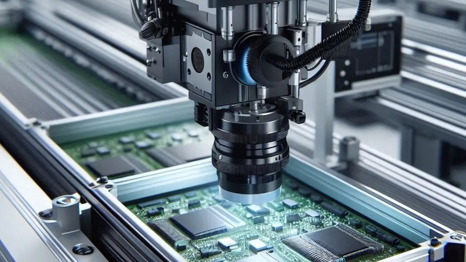
The Role of Edge AI in Inspection
Edge AI refers to deploying machine learning models on localized hardware rather than relying on cloud or data center processing. In semiconductor fabs, it means AI algorithms run directly on inspection machines equipped with specialized processors. These systems analyze high-resolution images in real time, classifying anomalies as harmless variations or critical defects.
The advantage lies in both speed and autonomy. Because decisions are made on-site, operators no longer depend on external networks or remote servers. This independence ensures faster decision-making and provides resilience even if connectivity is interrupted. The result is a more efficient and self-reliant inspection environment.
Instant Feedback for Process Control
The ability to classify defects instantly has ripple effects throughout the fab. When inspection systems detect a pattern of defects, process parameters can be adjusted on the fly. This feedback loop reduces downtime, optimizes yield, and prevents costly production delays.
For example, if a lithography tool introduces slight alignment errors, edge AI can identify the resulting defects immediately and signal adjustments before more wafers are affected. In advanced manufacturing, where margins for error are nearly nonexistent, such responsiveness ensures consistent quality.
Precision in Classification
The strength of AI at the edge is not just speed, but accuracy. Machine learning models trained on vast libraries of defect images can distinguish between variations that impact performance and those that do not. It reduces false alarms that might otherwise slow production while ensuring critical flaws are flagged without delay.
As circuits shrink to nanometer scales, classification becomes more complex. AI’s ability to detect subtle, non-obvious patterns ensures fabs can maintain rigorous quality standards even as designs become more intricate. The combination of speed and precision makes edge AI indispensable for future manufacturing.
Enabling Predictive Insights
While real-time classification addresses immediate issues, edge AI also contributes to long-term process improvement. By aggregating insights from continuous inspection, these systems can reveal recurring defect patterns that point to root causes. This predictive capability helps fabs not only react faster but also prevent problems from arising in the first place.
As semiconductor manufacturing becomes increasingly connected, IoT and AI/ML integration in semiconductor design is playing a growing role in enabling smarter monitoring systems, predictive maintenance, and data-driven process optimization across fabrication environments.
When paired with predictive maintenance, edge AI creates a manufacturing environment where defects are anticipated and avoided rather than managed. This proactive approach reduces downtime, extends equipment life, and maximizes throughput.
Precision Without Delay
The integration of AI at the edge is particularly transformative at the nanoscale, where inspection speed must not come at the cost of accuracy. Erik Hosler explains, “The ability to detect and measure nanoscale defects with such precision will reshape semiconductor manufacturing.” His insight illustrates why real-time classification is vital: accuracy and speed together define success in advanced fabrication.
By providing immediate clarity, edge AI empowers fabs to maintain both precision and efficiency, ensuring that rapid inspection does not sacrifice quality. This balance is critical as the industry advances toward ever-smaller nodes with more demanding requirements.
Broader Industry Benefits
The adoption of real-time defect classification has broad implications across industries. In automotive manufacturing, it ensures chips powering safety-critical systems are flawless and reliable. In consumer electronics, faster inspection cycles support higher production volumes without compromising quality.
Data centers and AI hardware vendors also benefit, as real-time defect management improves consistency in high-performance chips. With global demand for semiconductors rising, edge AI helps ensure manufacturers can scale production responsibly while maintaining rigorous quality standards.
Overcoming Challenges to Edge AI
Despite its advantages, implementing edge AI for wafer inspection comes with challenges. Hardware capable of running advanced AI models must be embedded in inspection tools, which requires investment and integration with existing systems.
Another barrier is model training. AI systems must be trained on massive, high-quality datasets to classify defects accurately. Collecting and curating these datasets is resource-intensive, and ensuring models generalize well across different fabs and processes remains a technical hurdle.
Security is also a consideration. Processing data at the edge reduces exposure, but models themselves may contain valuable intellectual property that must be safeguarded against theft or misuse. Addressing these concerns is essential to enable broader adoption.
Toward Instant Insight in Manufacturing
Real-time defect classification powered by edge AI is ushering in a new era of responsiveness in semiconductor manufacturing. By moving intelligence directly to the point of inspection, fabs can identify and resolve issues the moment they arise. The combination of immediate feedback, predictive insights, and nanoscale precision redefines how quality is maintained in advanced fabrication.
As the industry pushes toward ever-more complex chips, edge AI will serve as a cornerstone of smart manufacturing. Instant insight will not only protect yields but also drive innovation, ensuring that semiconductor fabs remain agile, efficient, and prepared for tomorrow’s demands.